Simulation Tools, Real Components and Limitations
By Bryan Ackerly, VK3YNG
Abstract
In recent times there have been a number of software
manufacturers who have made affordable, or even free, simulation software
available to amateurs. Although many of these free tools are cut down versions
of much more powerful packages, they still allow simulation of many real
world circuits that would have been well beyond the means of many amateurs
only a few years ago.
To make proper use of these tools, an awareness
of their limitations is required. This paper outlines some of the tools
available and some tips on getting effective use from them.
1. Introduction
In the past high frequency simulation tools were
only available to relatively large commercial engineering concerns. These
software tools were extremely expensive and in many cases required a large
amount of equally expensive training to make effective use of them.
In recent times a number of companies have released
cut down evaluation or student versions of some very good simulation
tools that in most cases are available free of charge from the companys
web site. These tools are a lot more user friendly than their predecessors
and provided some understanding of the limitations involved is taken into
account, these tools can provide very close approximations to real world
designs to the point where trimming a final design is unnecessary. This
paper concentrates on getting effective use from these free tools.
2. Why simulate
Simulation tools are an invaluable design aid which
allow concepts to be tried out without having to spend many hours trying
to coax a physical circuit into operation. They are also very useful as
a learning tool and allow the experimenter to quickly see the effects of
changing various circuit components in an otherwise working design.
You can, for example, determine if a circuit is
stable and what needs to be done to make it that way rather than finding
out when you build it for the first time and let all the smoke out. Existing
designs that were done before the availability of these tools can be further
optimised for one or all of gain, return loss or noise figure for example
using real components.
These modern tools are also a lot more user friendly
allowing you to get up and operational without needing several days or
weeks of training on how to use the tool. However, the tools still require
some fundamental understandings of what you are working with and the old
adage of Garbage in = garbage out still applies.
3. Types of simulation
3.1 Linear Simulation:
Linear simulation is used to simulate small signal
performance of circuits and assumes there are no bounds on signal levels
or linearity. Linear analysis allows the modelling and optimisation of
input and output return loss (VSWR) amplifier forward and reverse small
signal gain, stability and noise figure. Active and passive lumped and
distributed circuits can generally be modelled and optimised.
3.2 Non-linear simulation
Non-linear simulation is useful for determining
intermodulation performance and compression levels of linear and non-linear
amplifiers and for modelling oscillators and mixers. Many free simulation
tools offer a small range of non linear models for common active devices.
Unlike linear simulation where models are commonly available in the form
of S-parameters, non-linear models are usually proprietary and a lot more
difficult to obtain.
3.3 System simulation
System simulation is useful for analysing and optimising
the performance of cascaded major functional blocks in an Analog or Digital
RF communication system. System simulation is beyond the scope of this
paper but could prove very useful for those who are interested in the bigger
picture.
4. The mathematics behind
4.1 Methods of simulation
There are several methods used inside simulation
tools. An analysis of these is beyond the scope of this paper, but briefly
the common methods used are:
Finite difference time domain, Finite element
method, Method of moments and Method of lines.
4.2 Types of simulation:
Simulation varies in its modelling ability and accuracy
due to tradeoffs in models used. Older software had to strike a balance
between the usefulness of the tool and modelling accuracy due to processing
and memory limitations. With increases in processing capabilities offered
by todays personal computers, the capabilities of modelling tools has
been able to increase to the point where very accurate results can be obtained
very quickly.
There are effectively three categories to these tools:
4.2.1 2D (infinitely thin tracks):
Some older simulators used 2D modelling to enable
equation based simulation which allowed minimal memory requirements and
usable results through the UHF range. In many cases however, the results
were somewhat limited.
4.2.2 2.5D (equation based)
Models box modes and track thickness. Most current
simulators currently fall into this category, including many which claim
to be 3D simulators. The modelling is equation based for the third dimension
rather than using full EM modelling and the effects of obstacles generally
cannot be taken into account.
4.2.3 3D (full space modelling)
This is presently the ultimate
simulator which models obstacles in full 3D using Maxwells equations. This
type of simulator is useful for waveguide and cavity filters and accurate
antenna modelling (Note that most of the tools that amateurs currently
use for Yagi design for example are based on interpolated tables and are
not true 3D analysis tools).
This type of simulator is the most accurate for
higher frequency and microwave use, but is extremely computationally intensive.
Generally, full 3D tools are used for analysis only rather than as an optimisation
and design tool due to the processing time, power and extremely large memory
requirements needed for accurate analysis.
5. Available Tools
5.1 Berkley Spice
This simulator has been around for a number of
years and many older implementations are public domain. More recent versions
of this simulator have found their way into commercial PCB and schematic
design packages like OrCad and Protel.
This simulator is good for modelling audio circuits and is particularly
good at modelling OpAmps. Many small signal transistors and basic integrated
circuits have spice models available for them. Spice is particularly good
for low frequency non-linear simulation and can give usable results through
VHF.
Pspice is also good for modelling HF oscillators
and some RF circuits and it is apparently possible to extract S-parameters
from spice models for devices where they are not supplied.
This is a 2.5D simulator
which is good for modelling rectangular elements, transmission lines, vias
in multiplayer boards and other 3D structures. The free version is limited
in memory which places some limits on the analysis but it is otherwise
a good tool for modelling EM behaviour in more than 2 dimensions.
It has a feature where
it generates colour plots of current density and is useful for modelling
many microwave components.
This is a very powerful
simulator which uses a script based programming language entry. This makes
it very useful for performing multiple simulations for comparing topologies
since multiple sets of directives can be generated and analysed simultaneously.
Aplac has lots of component
and stripline models, handles offset stripline and is very well documented.
This simulator may be difficult for a first time user due to its scripting
based nature but the package is becoming very commercial and graphical
front ends are apparently now available.
This simulator is one of the more recent simulators
to become available and is extremely powerful. It allows Linear and non-linear
harmonic balance simulation, Schematic capture, linear and non-linear circuit
and system analysis. An excellent overview of this tool was provided recently
in
QST [4]In particular it offers a facility called smith
tool which is very useful for designing impedance matching networks. Noise
and stability analysis is also offered and is fairly easy to use for those
who have understanding of how noise and stability are modelled using smith
charts.
Another very powerful feature of this software is
the ability to do tuning and linear optimisation. A set of goals are set
up and particular components can be targeted to optimise a circuit to achieve
desired results. There are a number of different optimisation methods available.
Serenade includes Models for basic transmission
lines, edge coupled transmission lines (useful for microstrip filters),
open ended lines and optimally mitred bends.
The student version has limitations which include:
- 25 circuit elements
- 1001 sweep points
- 4 probes
- 2 DC bias sources
- 4 non-linear device ports
- 31 spectral components (useful to 5th order)
- 2 fundamental tones
Of all of these, the 25
circuit elements is the biggest limiting factor when trying to optimise
a circuit with real components. However, there are ways of getting around
this problem by selective use of S-parameter or ideal component models.
5.5 Other tools
This list is by no means complete. New tools are
being made available and some older versions are becoming freely available
via the Internet. Of interest recently has been an extremely powerful tool
called
Microwave Office 2002. The
capabilities of this tool are very impressive. It will be interesting to
see if the company releases an entry level version of this tool, but they
do offer free trials of their software.
6. Using simulation tools their limitations
Many simulation tools have limitations and understanding
them is crucial to get the most out of the tool. For modelling circuits
in the HF through low VHF spectrum the effects of wires and PCB tracks
can often be ignored without major impact provided Qs are low and the
design is relatively compact. For modelling high VHF through microwave,
transmission lines and PCB tracks must be included.
Generally most simulation tools are usable to around
6 to 10GHz. Above these frequencies, physical structures start to become
less than ideal and it becomes increasingly important to model structure
geometry, imperfections and proximity effects in full 3D using maxwells
equations.
7. Components
In order to gain the best results from VHF and up
an understanding of the operation and limitations of components at RF frequencies
is paramount.
For most designs in the VHF through low microwave
frequencies, if the results didnt agree closely with the simulation then
there is either a mistake somewhere in your design or there is a parameter
that has been oversimplified or left out of the simulation. Even millimetre
long lengths of track can make a difference as the frequency goes up.
7.1 Why use surface mount components?
Possibly the most important rule of any successful
simulation is that the component models are accurate. At HF frequencies
it is possible to disregard lead inductances and other parasitic effects
as their contributions are generally minimal.
As frequencies increase through VHF and beyond,
component leads and termination methods contribute a growing uncertainty
to measurement that is difficult to predict and can severely limit the
accuracy of results if ignored.
Surface mounted components on the other hand are
predictable and consistent and are often supported by manufacturers models.
Connections are usually done through PCB tracks which can also be modelled
accurately giving accurate results even through microwave frequencies.
7.2 Resistors
Surface mount resistors are accurate to many GHz.
The lowest and highest resistors tend to depart from their marked values
through parasitic effects. Low resistance values tend to be dominated by
series inductance while high values begin to get swamped by parallel capacitance.
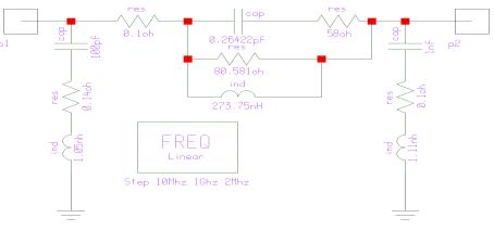
A simple resistor model has been determined through
measurement and is shown in figure 1.
7.3 Capacitors
For low RF and audio frequencies, capacitors can
be used as if they are ideal components provided the ESR is not important.
As frequencies increase, series inductance plays an increasing role and
the ultimate capacitive reactance is limited by series resonance.
Since some larger ceramic capacitors start to become
self resonant in the low megahertz, this parameter cannot even be ignored
at HF frequencies.
Table 1 shows some actual measurements of capacitor
self resonance and ESR performed on a calibrated Vector Network Analyser.
Of interest is that in nearly all cases the equivalent series inductance
is around a nanohenry. The surprise was that the very tiny 0402 components
possessed similar self inductance to larger 0603 and 0805 case styles.
This table shows the claim that smaller components possess lower parasitics
appears to be unfounded.
Table 1 - Capacitor Self Resonance
Measured on HP8753ES Network Analyser.
|
Capacitor Value (size) & type:
|
ESR (ohms)
|
Self Resonant Frequency (MHz)
|
ESL(nH)
|
Notes:
|
|
1pf (0603)
|
0.65
|
5300
|
0.90
|
|
|
2p2 (0603)
|
0.63
|
3400
|
1.00
|
|
|
3p3 (0603)
|
0.43
|
2860
|
0.94
|
|
|
4p7 (0603)
|
0.46
|
2160
|
1.16
|
|
|
5p6 (0603)
|
0.36
|
2025
|
1.10
|
|
|
5p6 (1206)
|
0.7
|
2100
|
1.03
|
|
|
6p8 (0603)
|
0.46
|
1820
|
1.12
|
|
|
6p8Q (0805)
|
0.3
|
1940
|
0.99
|
High Q
|
|
10p (0402)
|
0.42
|
1570
|
1.03
|
|
|
10p (0603)
|
0.42
|
1530
|
1.08
|
|
|
10p (0805)
|
0.3
|
1640
|
0.94
|
|
|
22p (0603)
|
0.33
|
980
|
1.20
|
|
|
22p (0805)
|
0.28
|
1080
|
0.99
|
|
|
33p (0603)
|
0.52
|
850
|
1.06
|
|
|
47p (0603)
|
0.31
|
730
|
1.01
|
|
|
47p (0805)
|
0.43
|
776
|
0.89
|
|
|
100p (0603)
|
0.14
|
490
|
1.05
|
|
|
220p (0603)
|
0.15
|
350
|
0.94
|
|
|
470p (0603) C0G
|
0.13
|
240
|
0.94
|
|
|
470p (0805) C0G
|
0.11
|
240
|
0.94
|
|
|
470p (0603) X7R
|
0.92
|
280
|
0.69
|
|
|
1n (0603) X7R
|
0.42
|
173
|
0.85
|
|
|
1n (1206) NP0
|
0.1
|
151
|
1.11
|
|
|
10n (0805) X7R
|
0.16
|
61
|
0.68
|
|
|
10n (0612) X7R
|
0.49
|
168
|
0.09
|
Special low ESL capacitor
|
|
100n (0805) X7R
|
0.07
|
14
|
1.29
|
|
|
1uF (0805) Y5V
|
0.07
|
4
|
1.91
|
Measured @ 0V (C=0.83uF)
|
|
1uF (0805) Y5V
|
0.06
|
7
|
1.08
|
Measured @ 5V (C=0.48uF)
|
|
68uF/6V (C)
|
0.165
|
0.6
|
1.03
|
Tantalum Measured @ 5V
|
The only major change was the special 0612 package
which is said to be designed for high frequency bypassing. This particular
component exhibited an order of magnitude lower series inductance and a
much higher series resonant frequency. The main reason for performing a
test on this device was to prove that stray inductance had been calibrated
out of the test jig.
ESR varies between about 0.05 to 1.0 ohms with lower
values occurring for the larger capacitance values and better dielectric
materials. NPO and C0G give much better results than X7R for example. Note
how both ESL and capacitance vary substantially with voltage in the Z5U
dielectric.
For simulation purposes, typically a capacitor can
be replaced with an equivalent series circuit comprising a capacitor of
the selected value, a resistor similar to that in table 1 and an inductor
of 1nH as shown in figure 2. This allows the capacitor value to be optimised
while taking into account its parasitic behaviour. In many cases either
or both of these parasitic components can be omitted, particularly for
coupling use but it is worth adding them and then replacing them with equivalent
short circuits once their contribution, or lack of, has been verified.
7.4 Inductors
Generally we are taught that capacitors can be treated
as ideal and inductors are very much a compromise due to mainly to limitations
of interwinding capacitance and wire resistance. The reality is that at
higher frequencies with smaller values the roles tend to reverse. Typically
small value (<100nH) surface mount inductors have self resonant frequencies
well into the Gigahertz region.
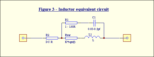
To accurately model these components with an equivalent linear model
is difficult since it involves modelling five components one of which varies
with the root of frequency. Equivalent parallel winding capacitance is
typically 0.1pf in series with a resistance (R1) that increases with approximately
the root of inductance and is typically 15 ohms for a 100nH
1008CS
inductor. Note that this is much higher than Rvar (typically = ESR) and
ultimately limits the self resonance Q.
|
Table 2 - Typical inductor ESR based on Coilcraft
1008CS
|
|
Inductance:
|
10nH
|
33nH
|
100nH
|
330nH
|
1uH
|
|
min SRF (MHz)
|
4100
|
1600
|
1000
|
570
|
290
|
|
Cp(pf)=
|
0.13
|
0.145
|
0.17
|
0.158
|
0.217
|
|
typ SRF (MHz)
|
4414
|
2301
|
1221
|
697
|
342
|
|
K=
|
2.00E-05
|
5.00E-05
|
1.35E-04
|
3.80E-04
|
1.20E-03
|
|
Freq=
|
ESR=
|
ESR=
|
ESR=
|
ESR=
|
ESR=
|
|
0
|
0.08
|
0.14
|
0.56
|
1.05
|
1.75
|
|
10
|
0.11
|
0.16
|
0.43
|
1.20
|
3.79
|
|
50
|
0.19
|
0.35
|
0.95
|
2.69
|
8.49
|
|
100
|
0.25
|
0.50
|
1.35
|
3.80
|
12.00
|
|
200
|
0.33
|
0.71
|
1.91
|
5.37
|
16.97
|
|
400
|
0.45
|
1.00
|
2.70
|
7.60
|
*
|
|
1000
|
0.68
|
1.58
|
*
|
*
|
*
|
|
1400
|
0.80
|
1.87
|
*
|
*
|
*
|
|
2000
|
0.94
|
*
|
*
|
*
|
*
|
|
2500
|
1.05
|
*
|
*
|
*
|
*
|
|
* = impedance limited by self resonance
|
|
|
Effective modelling can be done using a discrete ideal
inductor to simplify initial design and optimisation and then replace it
with an S-parameter equivalent for final analysis and tweaking. If ESR
is important table 2 can be used to model this parameter at the frequency
of interest. In many cases this parameter can be omitted, but it is wise
to include it initially. Note that this technique only works when the inductor
is used well below self resonance. Near resonance the S-parameter equivalent
model is recommended, but this usually excludes the part from automated
optimisation.

Many reputable inductor manufacturers provide S-parameter
equivalent circuits via their web sites. For small values, final tweaking
can often be performed in simulation by altering the track length to the
inductor once the ideal inductor has been replaced with its S-parameter
equivalent.
7.5 RF Beads
These devices are often used as a cure all and
after doing some measurements it appears their effectiveness is somewhat
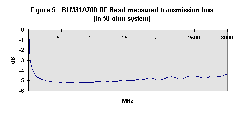
overrated. Figure 5 shows the transmission loss of a typical 500MHz RF
bead. Note that the transmission loss is typically in the order of only
5dB in a 50 ohm system, hardly the earmarked 40 plus dB that many users
of these devices expect.
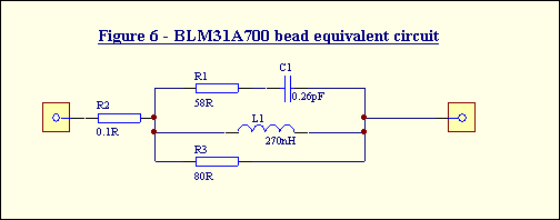
These devices can be modelled
as a well damped (low Q) RLC parallel circuit. Figure 6 shows a derived
equivalent circuit for the Murata BLM31A700 RF Bead. Note that this circuit
only holds for zero bias as these devices are also somewhat dependant on
the current going through them.
Generally beads with higher impedance have higher
Q and the attenuation falls off more rapidly either side of resonance.
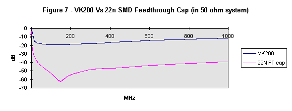
Figure 7 shows that even the popular 6 hole VK200
beads only possess an insertion loss of 19dB at resonance (120MHz) dropping
back to about 10dB at 1GHz. Contrast this with the attenuation measured
on an AVX 22nF W3F15C2238 surface mount feedthrough capacitor shown here
for comparison.

At first look it may appear that these devices are
not particularly useful. However, there is one particular application where
they can be used to particular benefit and this is to damp the parallel
resonance that occurs when two bypass capacitors of different value are
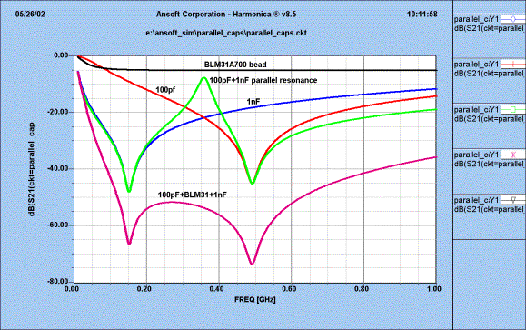
added in parallel. Figure 8 shows the effect of paralleling two real
C0G bypass capacitors. This is often done to so called broadband bypass
filtering. Note the peak in the attenuation response at 360MHz. This peak
is 14dB worse than the attenuation at this frequency of either capacitor
on its own! Such a peak can be the source of instability problems if it
is not taken into account. Parallel capacitors can be very problematic
if their effects are not properly understood.

Figure 8 - parallel bypass capacitors
Note the lower trace on
figure 8 which is the combination of the two parallel capacitors separated
by a ferrite bead. The series resonance points of each capacitor are still
evident but the parallel resonance between the two has been significantly
damped. Note also that the overall attenuation is more than 20dB better
at all frequencies and is also far better than the bead on its own. Loss
at near DC frequencies is minimal. Figure 9 shows the equivalent circuit
of these three components used for this simulation.
Figure 9 - bypass capacitor simulation
7.6 Active devices
Simulation tools generally contain a rather large
number of well characterised linear and non-linear active device models.
Where linear models are not included with the simulator they can usually
be obtained from manufacturers web sites or by contacting the device manufacturer
and requesting them. Linear models are generally provided in the form of
S-parameter (.S2P) files.
Some manufacturers also provide optimal noise match
data in these files. If this data is not included the device is assumed
noiseless and the modelling will only show the contribution of added noise
due to losses in matching components. If you are interested in accurately
optimising noise figure of an amplifier check that there are two lines
towards the end of the S2P file containing something like the following:
!FREQ Fopt
GAMMA OPT RN/Zo
!GHZ dB
MAG ANG -
Non-linear models are generally proprietary and
the tool designers will charge many thousands of dollars to create them.
If you are interested in modelling intermodulation or compression points
or designing non-linear amplifiers or oscillators, make sure the device
you intend to use exists as part of the tools non-linear components library.
7.7 PCB tracks
For a successful design to be properly modelled,
information on the PCB tracking should be included. Most simulation tools
provide this facility and have facilities to include one or more substrates
in Microstrip or symmetrical stripline structures. Some tools may offer
limited support for offset stripline.
It is vital to have some information about the dielectric
constant and tangent loss characteristics of the PCB material used. Typically
standard FR4 has a dielectric constant of around 4.4 at UHF frequencies
due to currently used levels of glass resin. The old standard of Er=4.7
is only really applicable at very low frequencies and it generally drops
as the frequency increases[8]. Tangent loss of FR4 is typically around
0.05. If in doubt consult manufacturers datasheets. FR4 can be used through
to microwave frequencies provided careful attention is paid to keeping
Qs low and minimising lengths of unnecessary transmission lines.
Teflon dielectrics have better controlled dielectric
constants and tangent loss of 0.005 or better. Newer Composite dielectric
materials also offer Teflon like characteristics at much better prices
and the manufacturability of FR4.
8. A sample design
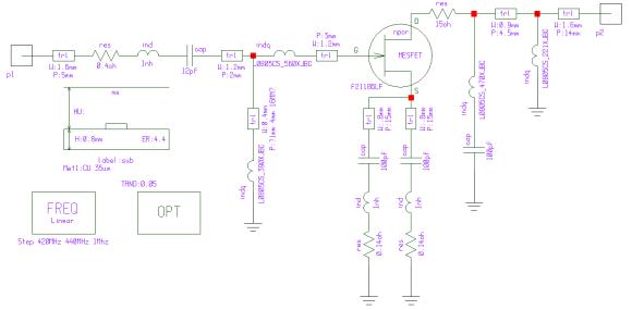
A 70cm amplifier was built using the Ansoft Serenade design
tool as shown in figure 10. This circuit uses an ATF21186 GaAsFET in a
self biased configuration. A 0.8mm thick FR4 laminate was used
Figure 10 - 70cm preamplifier simulation
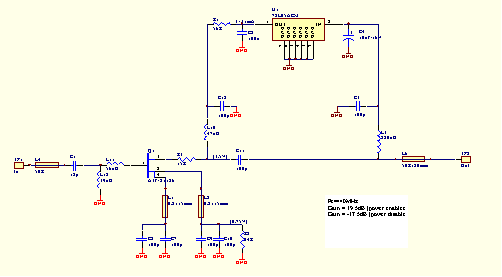
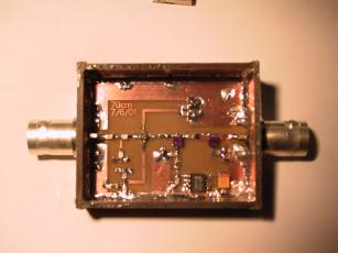
A schematic was then developed and a PCB using Protel as shown in figures
11 and 12. This particular amplifier was designed to be phantom powered
(i.e. power supplied via output coax connection)
Figure 11 70cm Preamplifier Schematic
Figure 12 70cm Test Preamplifier
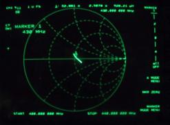
Figure 13 measured input match
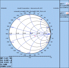
Figure 14 Simulated input and output match.
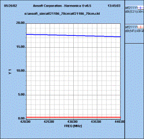
Figure 15 Simulated Gain and Noise Figure.
Actual measured performance was comparable to
that simulated with the input impedance measuring 53.5+j3.88 ohms (figure
13) compared to the simulation result of 56.5+j1.7 ohms at 430MHz (figure
14). Measured gain was also slightly higher than predicted measuring at
about 19.4dB where the simulation result was 17.48dB (figure 15). This
difference in gain has been attributed to the drain source voltage being
somewhat higher than the model due to self biasing.
Noise figure was measured at 1.6dB although this
is difficult to compare with the simulation as there was no noise data
in the model. The simulation tool predicted 0.42dB of added noise figure
due to component losses indicating a device noise figure of 1.2dB. It should
be noted that the optimisation was set to obtain a target gain of more
than 15dB, input and output return loss of better than 13dB and an added
noise figure of less than 0.5dB. Although source degeneration was used
in an effort to try to obtain simultaneous noise match and input match
while sacrificing some gain, the noise figure result is probably not optimal
due to the lack of optimal noise match data. In any case the results are
quite usable as far as a demonstration of the design tool is concerned.
There was no tweaking of any components in the final design.
9. Test equipment
Test equipment can form a very useful method of
validating a design. Here are some devices which may prove useful, however
a full description of test and verification methods is beyond the scope
of this paper.
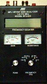
9.1 The MFJ SWR analyser:
Figure 16 - The MFJ 259
SWR Analyser
This device is claimed
to measure impedances between 7 and 650 ohms. But measurements (tested
with the B version) become inaccurate near these limits and even properly
calibrated 50 ohm loads become somewhat inaccurate as the frequency of
measurement increases. Also there is no sign for the reactance so it is
difficult to determine if the load is inductive or capacitive. Both open
and short circuits tend to read as a real resistance of zero ohms.
This unit has limited ability
to measure one port S-parameters at HF frequencies and some self resonance
parameters can be determined for larger components provided accurate ESR
measurements are not required.
9.2 Vector Network analyser
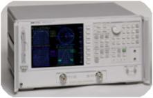
This is an extremely useful
device for characterising RF circuits and devices. It can accurately measure
complex impedance from milliohms to tens of kilo ohms and sweeps from tens
of KHz through to around 40GHz depending on the instrument. Unfortunately
even older base model units on the secondhand market still attract prices
starting at well over US$10,000 putting them out of the reach of most amateurs.
Figure 17 the
Agilent
8753ES Vector Network Analyser
9.3 A Cheap network analyser?
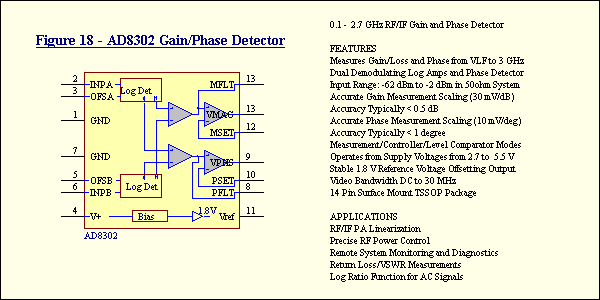
Recently,
Analog
Devices released a device called the AD8302 gain and phase detector.
This device performs two port measurement of relative gain to within +/-30dB
and phase accurate to 1 degree at frequencies up to 2.7GHz. Paired up with
a good directional coupler and a suitable swept or even manual frequency
source, this device could perform some very useful device characterisations.
The author is considering a project based on this device for a future Gippstech
presentation.
10. Conclusion
Software simulation tools allow amateurs to test
out circuits and scenarios quickly and easily and take a lot of the guesswork
out of circuit and system design. When teamed with surface mounted components,
which in many cases are accurately modelled by manufacturers data, a designer
can try out what if scenarios quickly and accurately predict the performance
of an RF circuit before construction.
With the aid of these new design tools and the availability
of well characterised components, the task of designing higher frequency
or microwave RF circuits has never been easier. These are empowering tools
and many of them are free. Use them!
11. References:
The author would also like to thank Richard Gipps,
from Trio Datacom for invaluable guidance in use of simulation tools and
their limitations.


