
Figure 4 – Solid Tungsten drill and router bits
 The Kinsten PCB material is available from several Australian
suppliers (2
,3
,4
,5
) in the following formats:
The Kinsten PCB material is available from several Australian
suppliers (2
,3
,4
,5
) in the following formats: | Top layer draft: | Low resolution, flipped orientation |
| Bottom Layer draft: | Low resolution, normal orientation |
| Top Layer Final: | Highest resolution, film plotting, flipped orientation. |
| Bottom Layer Final: | Highest resolution, film plotting, normal orientation |

For the developing tray use a lid from an old floppy disk storage box. Don’t use acetone in this tray as it may attack the plastic.

Figure 3 - Kinsten ET10 etching tank from Kalex and Computronics
To consistently drill clean holes with sharp edges requires the use of
solid Tungsten drill bits that are commonly used by the PCB industry. There
are a number of suppliers (
4
,5
,8
) of these, but don’t expect to be able to get them from you local hardware
store or electronics hobbyist supplier. These drills are available in sizes
from 6.3mm down to 0.2mm but they are not cheap and the smaller ones are extremely
fragile. A reasonable bench press is required for these drills as any vibration
will destroy them. Use a spindle speed of around 7,000RPM for drill sizes
around 3mm and up to 28,000RPM for sizes around 0.7mm. These drill bits will
do around 10,000 holes before they go blunt and generally you will break
them before this happens. The drill bits shown in figure 4 are several years
old now and are still sharp even after many thousands of holes! Only consider
sharpening them if you have access to a diamond grinding wheel.
Figure 4 – Solid Tungsten drill and router bits
There are also "electroless tin plate" solutions available giving a dull tin finish. The trick to using this solution is to use distilled water rather than tap water as impurities in the water can compromise the plating results.
| 1) Create trackwork on the computer: This should always be done from the component side. Always be sure to include a border showing the final board outline. |
| 2) Print off a draft copy of the trackwork layers(s) as a check copy and a template for the film. Use the printer dialog box to select flipped artwork for the top layer. Make sure the "add holes" option is checked on your PCB software when printing. |
| 3) Cut out a piece of film approximately 20mm larger than the artwork. |
| 4) Stick this film down MATT (non-shiny) SIDE UP onto the paper with thin sticky tape. |
| 5) Put the paper back into the printer and print the artwork again using the Final print setting. Leave the film for a few minutes for the ink to completely set. |
| 6) Remove a sheet of Kinsten PCB from its packaging. With a pen, mark out two lines 3mm and 6mm larger than the required PCB, plus an allowance on one edge to hold the board in the etching tank. |
| 7) With the aid of a steel rule, cut along these lines with a Stanley knife and then carefully remove the thin 3mm strips of protective coating material. |
| 8) Cut through these exposed 3mm wide strips with a hacksaw. Be careful not to bend the board if using thin material as this damages the coating. |
| 9) File any burrs off. This is extremely important as any lifting of the film during exposure due to the board not being completely flat will cause registration problems. |
| 10) Remove the film from the sheet and cut off any remaining sticky tape. (Peeling it off will leave the glue behind.) |
| 11) Put the film dull side (printing side) up on the light box. Carefully remove the protective sheet from the PCB material and place it face down onto the film. |
| 12) Cover the light box and enable the UV light. Depending on light intensity this will take somewhere around 2 to 5 minutes. Use a digital "egg timer" to ensure that you don’t over expose the board. |
| 13) Remove the PCB from the exposure box and put it into the developing tray. Add a small amount of developer (enough to completely cover the board) and gently rock the board until the unwanted copper areas are completely free from resist) |
| 14) Remove and rinse the board. Keep the used developer for the time being. |
| 15) Hang the board in the etching tank. Depending on temperature and how used the etchant is, this may take anywhere from 5 to 15 minutes. It is a good idea to set the egg timer to about 10 minutes or so to ensure that you don’t over etch the board in case you get side tracked. Its rather difficult to put the copper back on!! |
| 16) Remove, rinse and dry the board. |
| 17) Place the board back into the light box and expose the board for the standard exposure time. |
| 18) Put the board back into the used developer and agitate it until all resist is gone. Discard the used developer. (These last two steps can be replaced by using acetone if time is critical) |
| 19) Drill the board and cut, file or route the edges to size. |
| 20) Spray the board with clear protective lacquer. (or plate with immersion tin coating) |
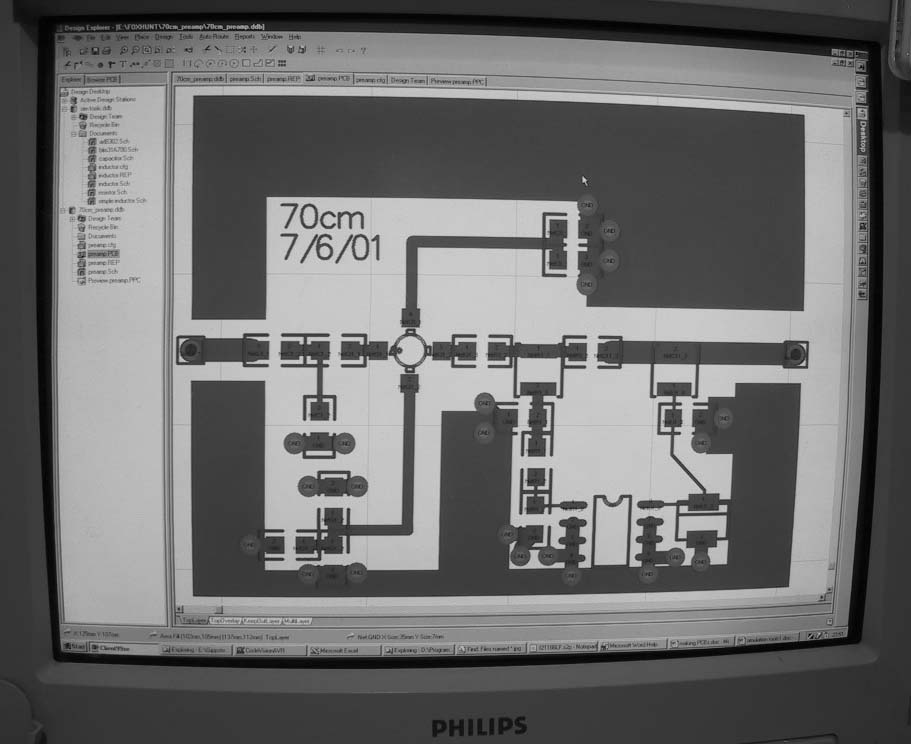
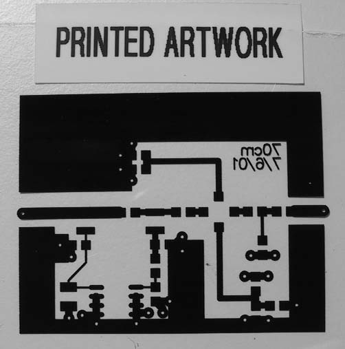
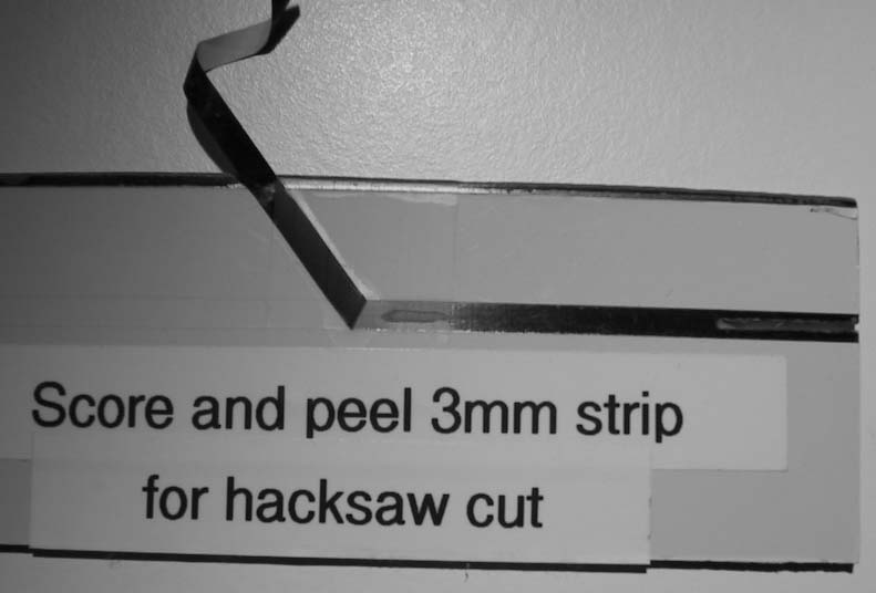
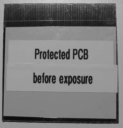
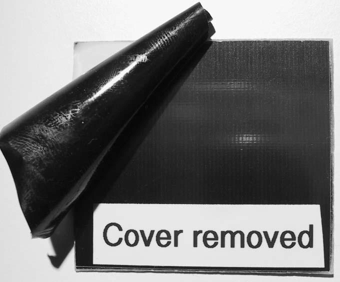
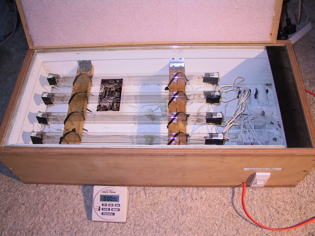
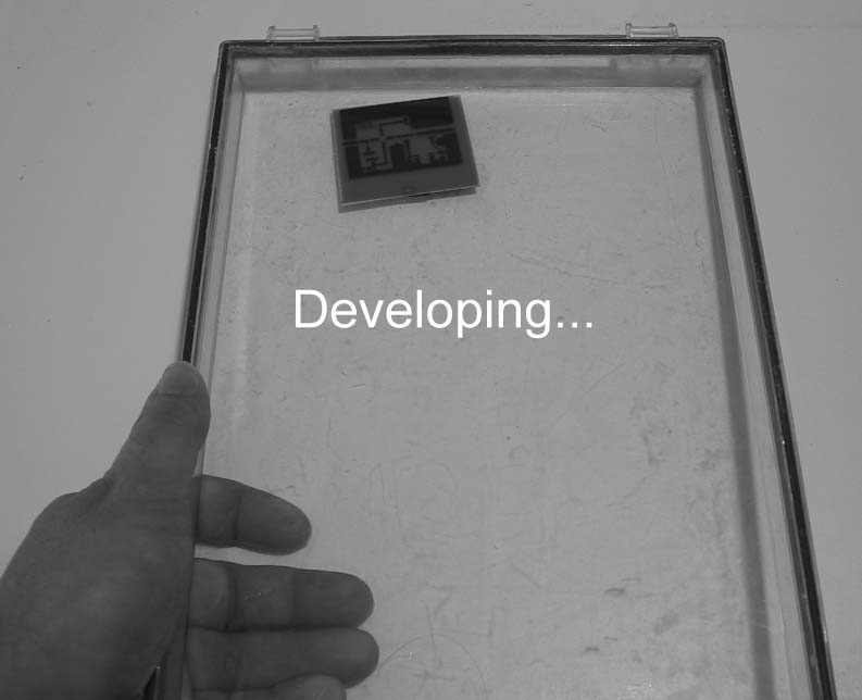
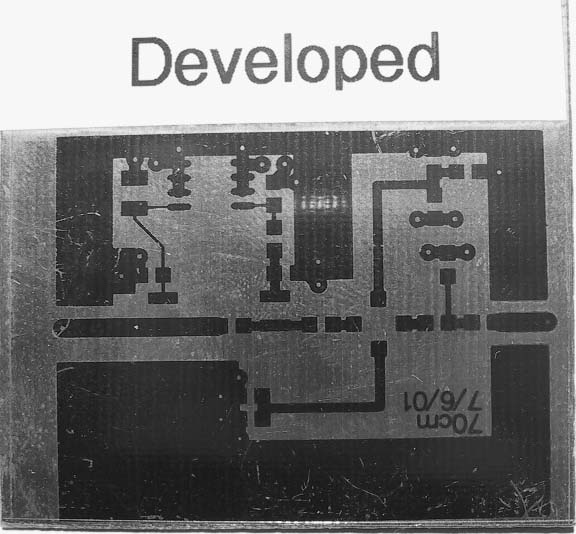
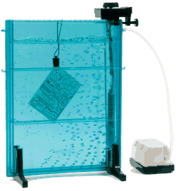
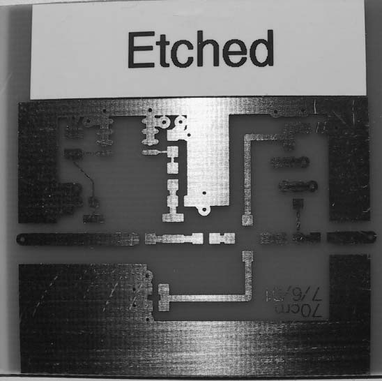
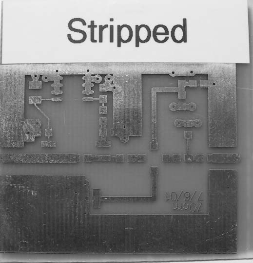
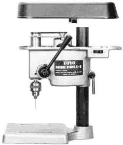
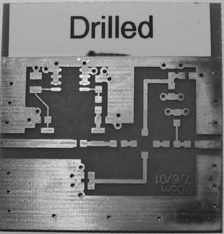
Figure 5 – various stages of making a PCB
And there you have it – The whole process once the board is designed should normally take around 10 to 20 minutes for a typical SMD board. (..or a bit longer for PTH boards because of all those damn holes). Artwork should be stored in a paper envelope to ensure that the ink doesn’t bleed onto other pieces of artwork and to avoid buildup of dust and fingerprints.
| 1) Tape one side of the artwork printing side up on a flat white surface. |
| 2) Put lengths of 3M double sided tape carefully along two intersecting edges about 1-2mm from the marked edge of the artwork. |
| 3) Get the other side of the artwork and carefully align it up with the first sheet. Use holes or board edge registration marks on three major edges for this purpose. (Make sure the alignment is correct and the you are holding the artwork firmly for the next two steps as you won’t get a second chance if you get it wrong!) |
| 4) Lift one edge of the artwork over the double sided tape and remove the protective cover from the tape. |
| 5) Carefully sit the top artwork over the double sided tape and tap it at few points to ensure it sticks. Don’t wipe your finger across it as this tends to make the tape "curl" |
| 6) Lift the other edge of the artwork and remove the cover from the other double sided tape. |
| 7) Carefully let the top artwork down and tap it in a few places to ensure it sticks. |
| 8) Put the PCB material inside this "artwork sandwich" for exposure. 1.6mm board should wedge quite firmly between the sheets so there should be no movement when the board is flipped to expose the other side |
| 9) When exposure has completed, put a folded blank piece of paper between the artwork sheets as otherwise the ink will tend to "bleed" from one side to the other over time making the artwork unusable. |
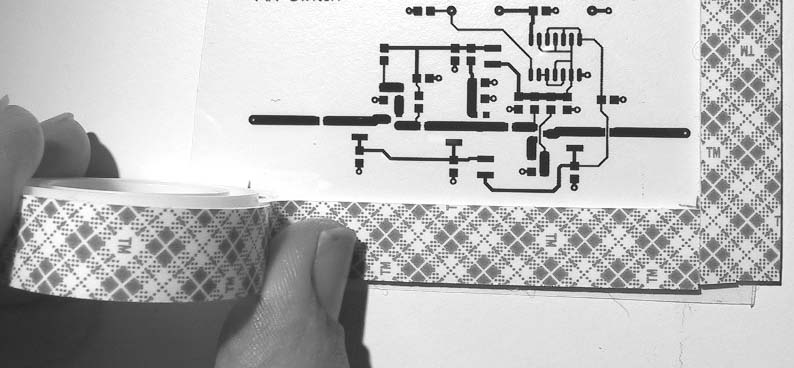
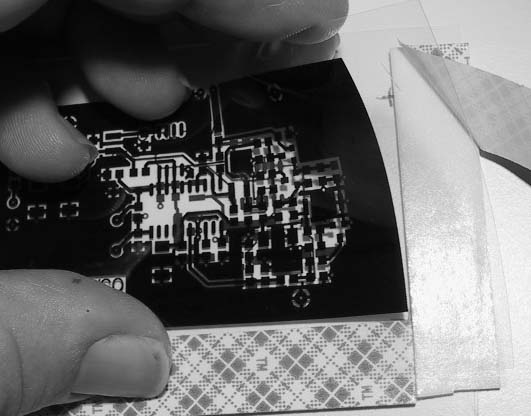
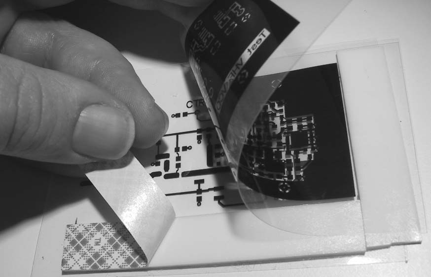
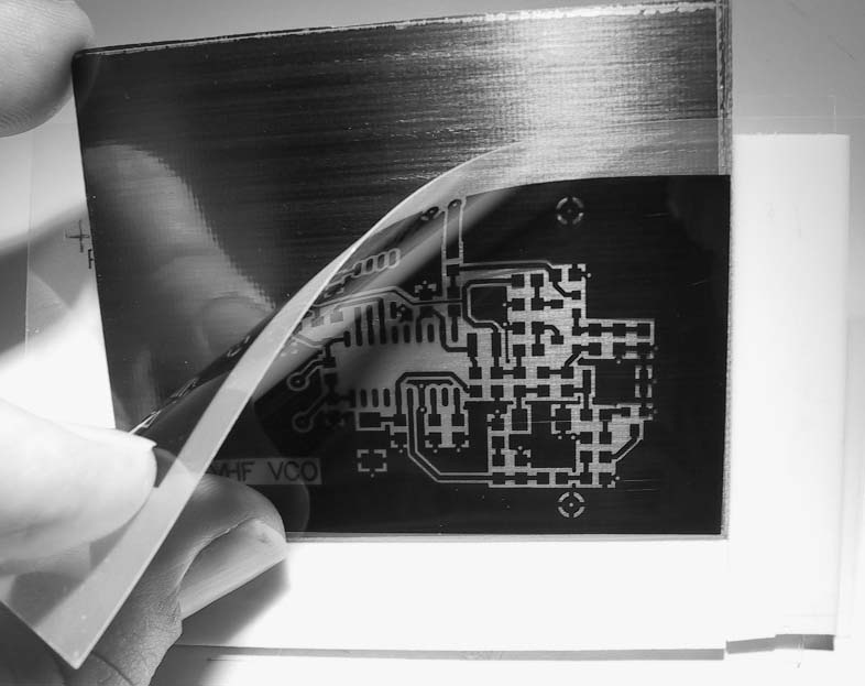
Figure 6 – Technique for double sided board artwork
2) Computronics Corporation , Bentley Western Australia
3) Wiltronics Research , Ballarat, Vic
4) Kalex Photosensitive Products 718 High St Rd, Glen Waverly, 3150. Ph +61 (0)3 9802 0788
5) Mektronics Co Pty Ltd , U3/67-71 Industrial Drive Braeside 3195.
6) Protel is a trademark of Altium Limited .
7) Epson Corporation ink jet printers
8) Farnell electronics
, Chester Hill, NSW